
|

|

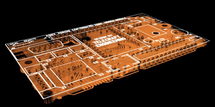
Throughout the early years of electronics, the printed circuit board (PCB) was thought to be merely the mechanical support for circuitry. However, in the new era of high frequency digital systems operating in the gigahertz range, circuit boards now play a critical role, and must be treated as a circuit component requiring considerably more design attention. In addition, electronic components have changed with the onset of new packaging technologies such as ball grid arrays and more miniature surface mount parts. Controlled impedance traces, increasing numbers of required logic voltages, and much smaller trace geometries have greatly increased PCB complexity. At Telecraft, we've embraced these new trends and have developed special measures for maximizing the performance of copper and dielectrics. We understand that the PCB is critical in the elimination of unwanted Electromagnetic Radiation (EMI), and have developed proven design methods for virtually guaranteeing first pass compliance for FCC EMI and EMC testing requirements. With designs, we sometimes must specify special dielectric materials, copper and layer thicknesses and other physical properties for the finished board to achieve a desired functionality. We perform impedance calculations, crosstalk analysis, and generate test models to determine optimum circuit trace geometries as well as including proper transmission line terminations as necessary to eliminate unwanted reflections. New higher speed digital designs require accurate control of trace lengths to control arrival times based on the propagation speeds of signals. 
Whether its power, analog, digital, RF, High Voltage, or a mixture, choose Telecraft for all of your printed circuit board layout and design needs. |